Cutting-edge technology lab opens in South Burlington
Vermont’s tech sector is getting a major boost with the official opening of a $3.4 million microelectronics lab in South Burlington.
Announcement
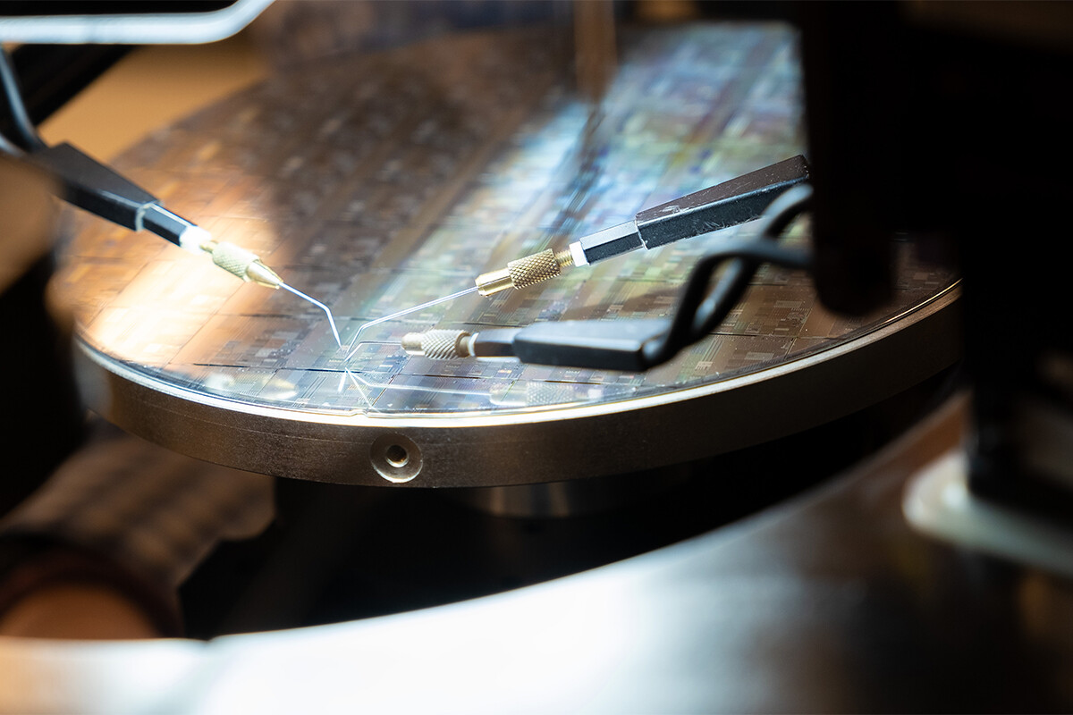
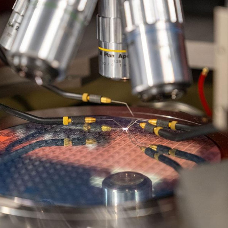
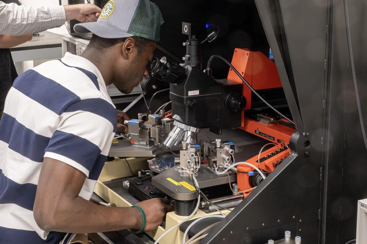
The Vermont Gallium-Nitride (V-GaN) Tech Hub opened its new Test and Characterization Facility, a major addition to the nation’s growing microelectronics innovation ecosystem and a critical resource for accelerating the transition of advanced semiconductor technologies from development to commercial deployment.

Mission
The V-GaN Tech Hub will build on Vermont’s culture of innovation by driving opportunities in education, research, and commerce that lead the development and commercialization of GaN Devices and spur vital workforce expansion across our region.
Vision
These semiconductors make products smaller, less expensive, and more energy efficient. That rise has fueled economic growth for the state’s companies in this sector and vocational advancement for their workers, as well as research and career preparedness opportunities across Vermont’s higher education landscape.
Comprehensive Technology Ecosystem
Vermont’s Tech Hub is one of six federal hubs awarded funding in this cycle. The investment will advance innovative projects in Vermont promoting GaN semiconductor technology, economic growth, and workforce development.
A cutting-edge facility offering start-ups affordable access to advanced GaN and semiconductor design tools, reducing financial risks and fostering innovation. Partnering with UVM’s Vermont Advanced Computing Center, and Enterprise Technology Services, the ADCC will support commercial and national security applications, driving next-gen computing solutions.
Located at OnLogic in South Burlington, V-GaN’s TCL will be the only publicly accessible lab in the U.S. offering comprehensive testing and technical advice for high-power and high-frequency GaN devices. Its capabilities were developed with input from key stakeholders, including GlobalFoundries, UVM’s College of Engineering and Mathematical Sciences, and smaller regional semiconductor firms.
UVM’s Professional and Continuing Education division will lead this major workforce development effort, offering K-12 initiatives to spark interest in GaN technologies, career pathways to increase rural access to semiconductor manufacturing jobs, and continuing education in semiconductor design, manufacturing, and GaN-specific skills. Partners include the Community College of Vermont, Norwich University, the Vermont State University System, and the Vermont Manufacturing Extension Center.
Latest
Vermont’s tech sector is getting a major boost with the official opening of a $3.4 million microelectronics lab in South Burlington.
New test and characterization facility will open to tech businesses and innovators in early 2026
UVM team develops program to introduce K-12 students to the rapidly expanding field of microelectronics Read the article here.
Latest News / 1.14.25
The Biden administration announced $23 million to fund Vermont’s Tech Hub. The Green Mountain State is pushing to be a leader in the production of next-generation gallium nitride, GaN, semiconductors.
Learn More
Experience the transformative power of innovation as Vermont leads the charge in revolutionizing semiconductor substrates. Discover how this paradigm shift is not only redefining the state’s technological identity but also propelling the semiconductor industry into a new era of efficiency and performance.
Doug Merrill
Regional Innovation Officer
Chris Boyer
Semiconductor Test Engineer
Mark Halfman
Northeast Microelectronics Coalition
Charlotte Bacon
Dartmouth College
Patrick Boyle
VMEC
John Cammack
KingCedar Holdings
Kevin Chu
Vermont Futures Project
Tricia Coates & Maureen Hebert
UVM
Kirk Dombrowski
UVM
Matt Dunne
Center on Rural Innovation
Nick Grimley
Vermont Agency of Commerce and Community Development
Jeralyn Haraldsen
UVM
Ezra Hall
Global Foundries
Joyce Judy
Community College of Vermont
Robert Sarkissian
Cadence
Phil Sussman & Sherman Patrick
Norwich University
Community
Sign up and join our community to discuss and help shape the future of Vermont as a technology and innovation hub. You’ll receive access to our community forum as well as regular updates via our newsletter.
Resources
Our Partners
If you have any additional questions or would like to reach out for more information regarding the Vermont GaN Tech Hub, please send us an email.
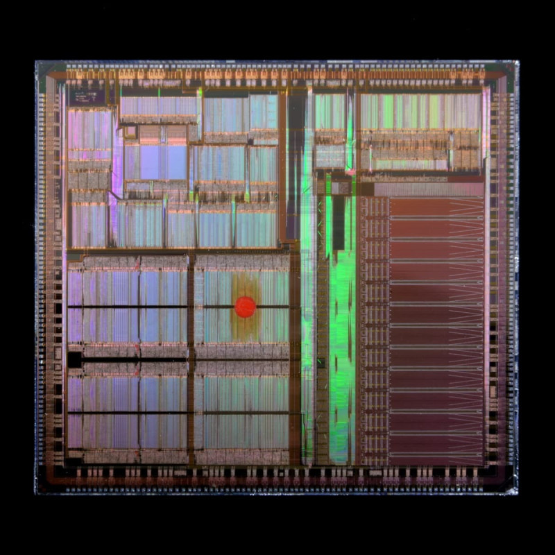
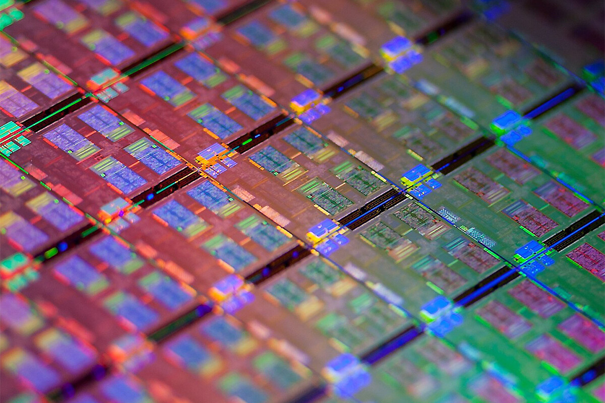
GaN is short for Gallium Nitride, a semiconductor compound. Semiconductor devices are built on substrates, think of the substrate as the dough disk below a pizza. Semiconductor devices that are built on GaN substrates have different properties than devices built on the more common silicon substrates, and these properties give them significant advantages in many applications.
GaN based semiconductors are in a class of materials called “Wide Bandgap Semiconductors” These materials can handle much higher voltage differences across them. This property makes them ideal for power conversion and motor controller applications. The first consumer product use of GaN devices is in the much smaller, but much faster wall chargers that mobile phone makers introduced about three years ago. Power devices made on GaN are smaller, more efficient, more powerful, and less expensive than equivalent devices made on traditional silicon.
The second property that helps GaN devices excel is known as ‘High Electron Mobility.’ Simply put, this means that the electrons in the atoms making up the semiconductor are not as tightly bound to their atoms as they would be in a silicon device. This property provides two valuable advantages. First, it results in more efficient transmission, meaning less heat production and higher electrical efficiency. Second, it means that GaN devices are capable of higher switching speeds, meaning that they can be turned on and off much faster than a traditional semiconductor. This makes them valuable for radio frequency (RF) devices like amplifiers and switches.
The US Department of Commerce’s Economic Development Agency launched the Tech Hub Program in 2023 to strengthen U.S. economic and national security with investments in regions across the country to make them globally competitive in the technologies and industries of the future. The program’s 31 Hubs will bring together diverse private, public, and academic partners into a collaborative consortium focused on driving inclusive regional growth.
Tech Hubs can apply for up to $75 million in grant funding by submitting proposals for projects in any of four eligible activities: workforce development, business and entrepreneur development, technology development and maturation, and related infrastructure activities. The Tech Hub will work with partner organizations to create projects and write proposals for up to eight projects by February 29, 2024. All projects must help the Tech Hub move toward fulfilling its mission. Organizations interested in creating or participating in a project should read the “Phase 2 Notice of Funding Opportunity (NOFO)” on this website.
If your organization has a project idea or believes it may be a useful partner in a project, please fill out our ‘Contact me’ sheet and we will follow up with you shortly.